Deposition
Adding a filmOnline
Material is added to the wafer a few atoms at a time; the method decides what the film can do.
At the WNF
SputterEvaporationALDPECVDOxidation


Learn how a chip is made, then spend a day inside the cleanroom where UW researchers and companies make real devices.
For students and working professionals · No prior knowledge required · Self-paced
Deposit, print, etch — then measure, after every step. A chip is that cycle repeated tens of times over, and those four steps are the four modules.
Four online modules, all required before the lab day. By the end you’ll be able to:
Material is added to the wafer a few atoms at a time; the method decides what the film can do.
The circuit pattern is put onto the wafer through resist, light and development — the step that sets the limit on everything else.
Wet chemistry or plasma removes what the pattern exposed; the profile you get is the whole point.
Thickness, alignment and dimensions are checked after every step, so a fault is caught before the next layer goes on.
Yes. There is no tuition, no fee and nothing to pay at any stage. The program is funded through a federal semiconductor workforce initiative; ChipReady.org and the University of Washington contribute the training, the facility and staff time. Your cleanroom suit, materials and lunch on the lab day are provided. Travel to Seattle and any overnight stay are your own arrangement.
Each is a recorded lesson from an instructor with exercises and a short quiz, about 30 to 45 minutes. All four take about three hours, spread however you like within your cohort’s window. You need 80% on each quiz, with two attempts; if you miss, you retake the module with no penalty. All four are required before the lab day.
You spend six to eight hours inside the cleanroom at the Washington Nanofabrication Facility, in a cleanroom suit, watching WNF engineers run the tools behind all four modules. The day opens with an hour of safety and logistics, then a morning session, lunch, and an afternoon session. Bring nothing but yourself. You must be 18 or older to enter the cleanroom.
Yes. About eight people can be inside the cleanroom at once and see the demonstrations properly, and lab days run roughly once a month. Enroll anyway — we place people in date order, and if the next lab day is full you go into the following one. We confirm your date by email.
On the University of Washington’s Seattle campus. Once your date is confirmed we send the building, where to arrive, and public transit options. Travel from outside the Seattle area is your own arrangement.
Neither, and we’d rather say so than oversell it. The program provides training and a certificate of completion; it does not include job placement and does not guarantee employment, interviews or referrals, and the certificate is not academic credit toward a UW degree. What it gives you is a working understanding of how chips are made, a day inside a professional cleanroom, and a certificate — specific experience you can point to on an application. And if you’re still deciding whether this industry is for you, it’s a good way to find out.
We use them to place you in a cohort, confirm your lab date and stay in touch. We report participation to the organization funding the program as numbers — how many enrolled, how many completed each part — never your personal details. We collect no demographic data and never sell your details. We share them only where the program requires it, such as with the WNF for cleanroom access. You’ll also be asked for a short survey after the modules and after the lab day; that is program evaluation, not research.
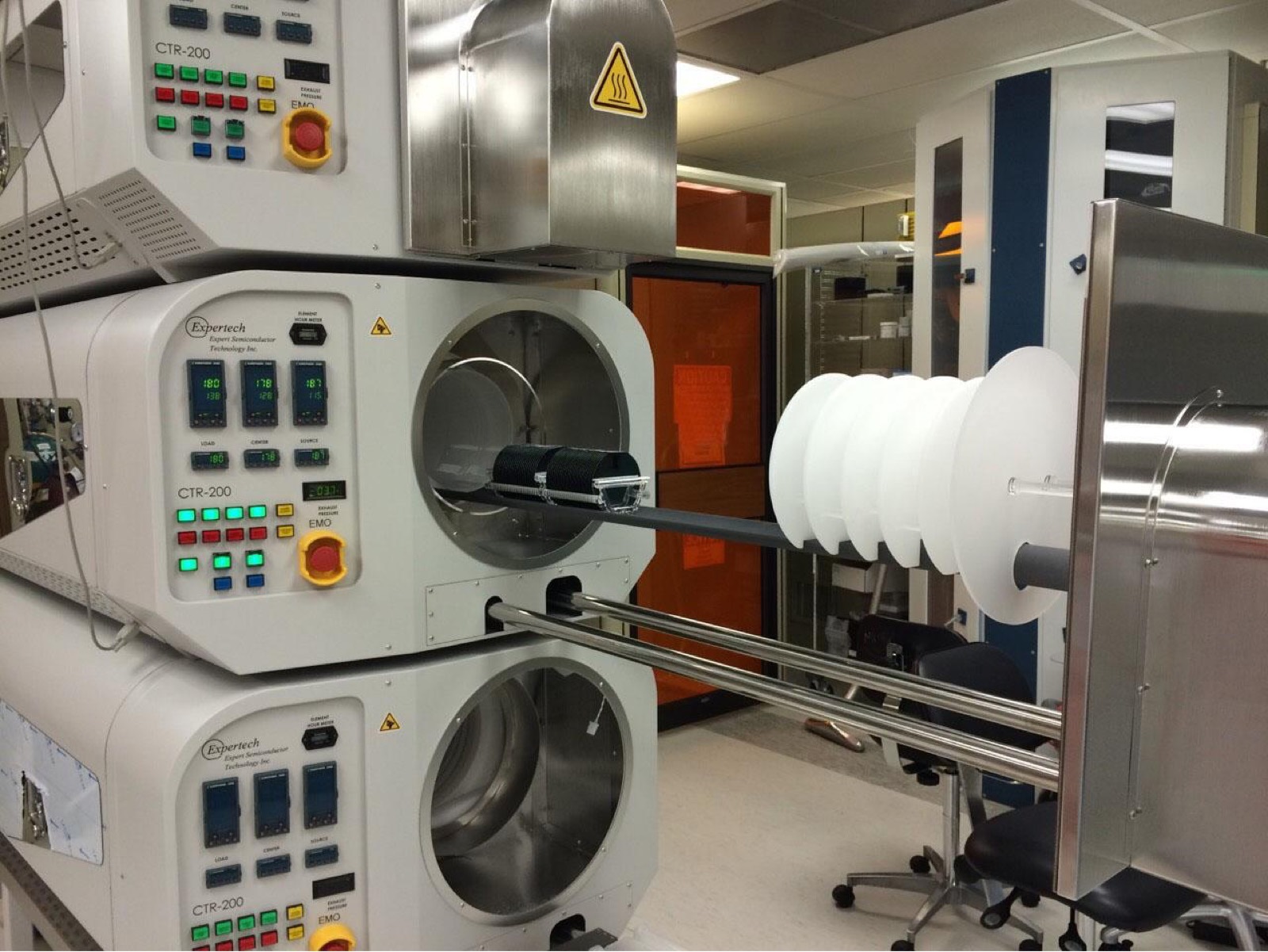
The cleanroom you would be standing in, and the tools you would watch being run. These are photographs of the facility itself.